BJT
Transistor Bias Voltage Calculator

See our other Electronics
Calculators.
The following calculators, will compute all of the
bias values of the transistor circuit, given the supply voltage, and the
base voltage, and all of the resistor values. The beta and Vd
transistor parameters, can be measured, or gathered from a data sheet. If
unknown, the default values below can be used, since the circuit is
normally fairly insensitive to these values.
This calculator also determines if
the transistor is in saturation or cut off, the frequency response,
and internal resistive and capacitive parameters for both the CE (common emitter) and CC
(common collector, also known as emitter follower) configurations.
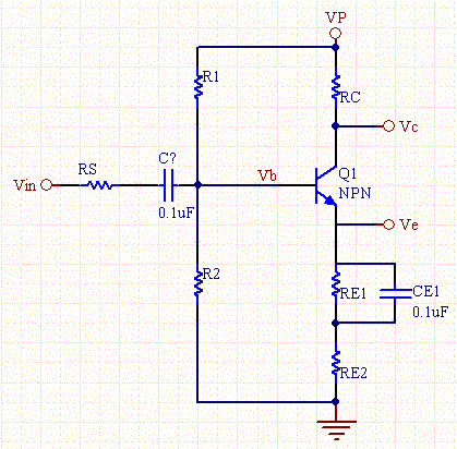 Transistor Biased with voltage divider
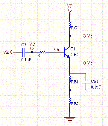 Transistor Biased with series resistor
DC biasing of a transistor is one of the
most common electrical engineering tasks. Transistors need certain
DC levels for them to function correctly. These DC are also know as
their bias point. Any AC signals which are injected into a
transistor circuit ride on top of these DC signals. Because of the
principle of linearity, the DC bias point and AC signals are design
independently. Another way of looking at bias is to measure what are
the DC values are at the various nodes within the circuit.
Depending upon how the transistor is biased
it can act as a switch or an amplifier, or buffer. When the transistor is
biased as a switch, resistor RE
is set to zero ohms (shorted out of the circuit), and the base voltage is
set to a level which saturates the transistor (turns it fully on).
For amplifiers, the input signal is usually
AC coupled through a capacitor to the bias resistor.
The common emitter configuration (class A
amp), is the most common type of amplifier transistor amplifier. The
input signal is injected into the base through a coupling capacitor, and
the output is taken off the transistor collector. The output signal is an
amplified and inverted version of the input signal. The output
signal typically can't swing the full range, because as the collector
current goes too high the transistor saturates, with the signal swinging
toward ground. Typically the base bias point is set to be about 1/3 of the
collector voltage. The emitter resistor is typically bypassed with a
large capacitor, so that it looks like a short to AC signals, otherwise it
reduces the gain of the AC signal.
The emitter follower is a buffer circuit,
which gives a gain close to 1. It is used because it has high input
resistance, and can provide good drive.
You may also fill in frequency information
for the transistor and it's nominal frequency operation point, and the
calculator will compute frequency dependent parameters, and the first pole
which limits the bandwidth of the amplifier.
Equations
Ib*Rb+Ib*Beta*Re+Vbe = Vin
Ib= (Vin-Vbe)/(Rb+Beta*Re);
Ic= Beta*Ib;
Ve= Ic*Re;
Vb= Ve+Vbe;
Vc= VP - Ic*Re;
If Vc<Ve the transistor is saturated.
if Vin< Vb the transistor is in cut off mode.
gm = Ic/25mA
rπ=
Beta/gm
fT=
gm/(2π*(CBE+CBC))
For the Common Collector:
RO=
RE || [re+(RB||RS)/(Beta+1)]
Rin= R1||R2||(rπ+(Beta+1)*RE2)
For the Common Emitter:
Ro= ~Rc;
Rin= R1||R2||(rπ+(Beta+1)*RE2)
Manufacturer Links
The best way to find electronic components is to use
our free Electronics
Component Directory, where a myriad of manufactures are
listed.
Other Electronics Links
We offer a broad range of electrical
engineering calculators and electronics
articles and tutorials.
Daycounter specializes in
contract electronics design. Do you need some help on your project?
Contact us to get a
quote.
[Employment]
[Downloads]
[Articles]
[Contact Us]
Salt Lake City, UT, USA
Disclaimer: Daycounter, Inc. doesn't guarantee the accuracy of any of it's content. Use at your own risk.
© Copyright 2016 Daycounter, Inc. All rights Reserved.
|