OSH Park
Shared projects
IMP003.v02
by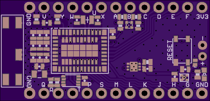
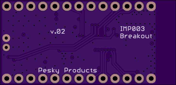
4
layer board of
1.46x0.71
inches
(37.08x17.91
mm).
Shared on
April 26th, 2016 03:42.
Significantly improved RF section, replaced pcb antenna with ceramic chip antenna, used 50 Ohm trace to antenna, and added 3V3 and GND at other board end.
Diode Board 2 - now with mounting holes
by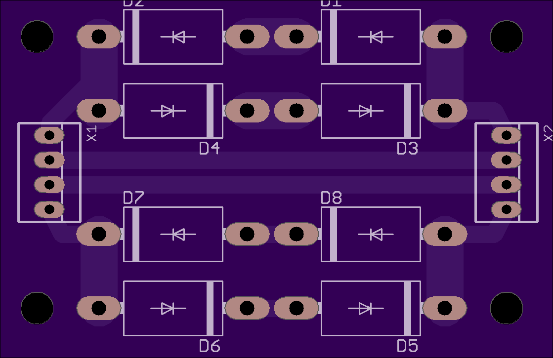
2
layer board of
2.24x1.45
inches
(56.82x36.83
mm).
Shared on
April 26th, 2016 01:51.
board for http://cabristor.blogspot.com/2015/02/drv8825-missing-steps.html
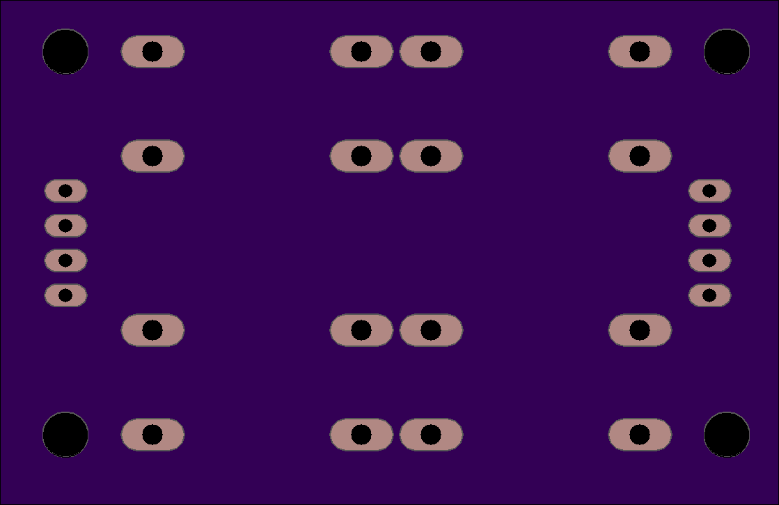
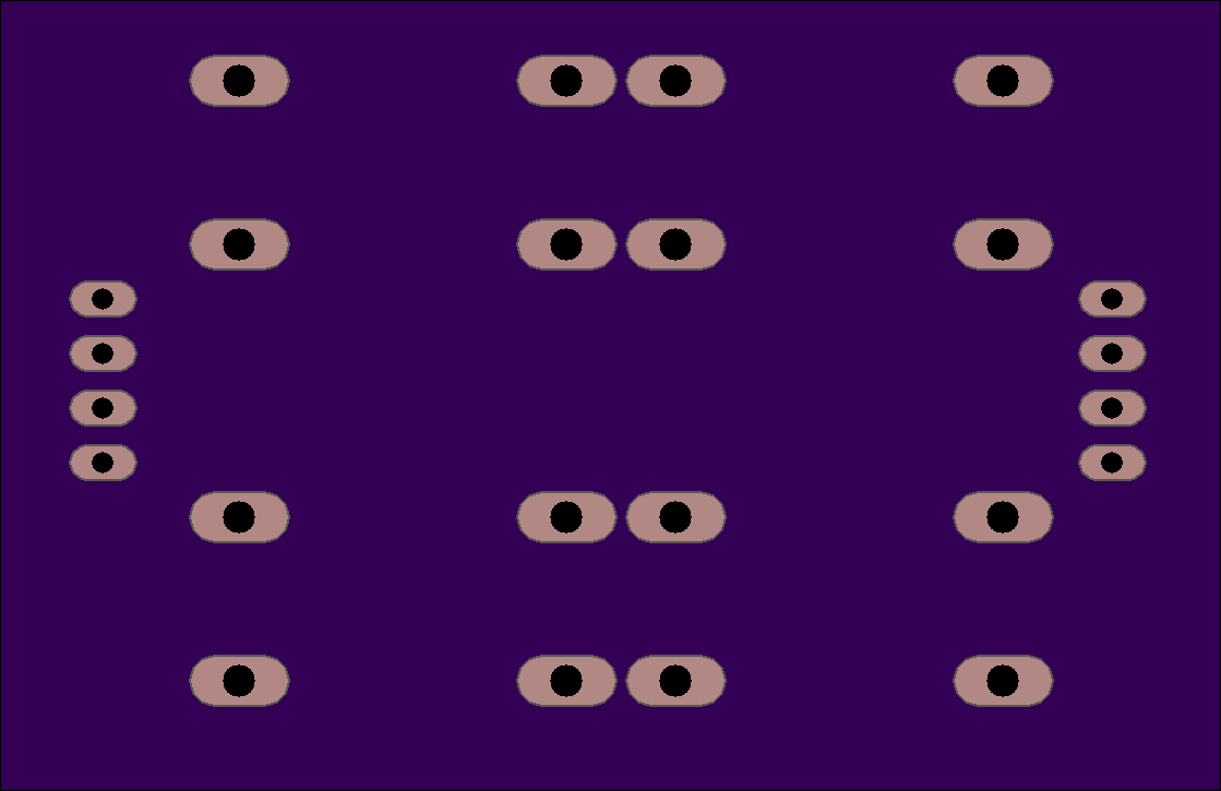
Diode mounting board
by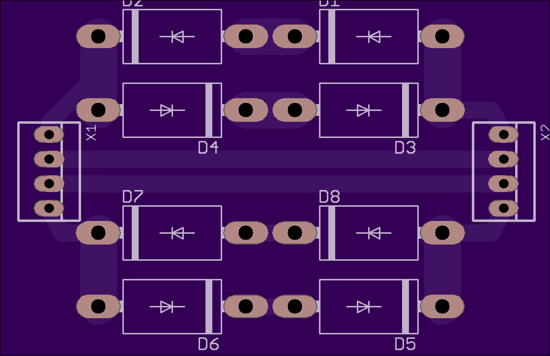
2
layer board of
2.24x1.45
inches
(56.82x36.83
mm).
Shared on
April 26th, 2016 01:47.
board for diodes to fix http://cabristor.blogspot.com/2015/02/drv8825-missing-steps.html
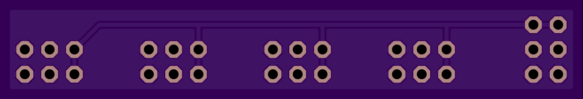
tt-i2c
by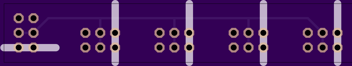
2
layer board of
2.35x0.40
inches
(59.72x10.16
mm).
Shared on
April 26th, 2016 00:06.
tt i2c mult
nRF52832_QFN48.v02a
by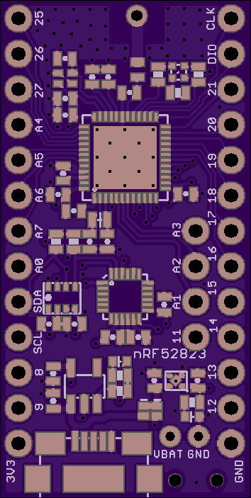
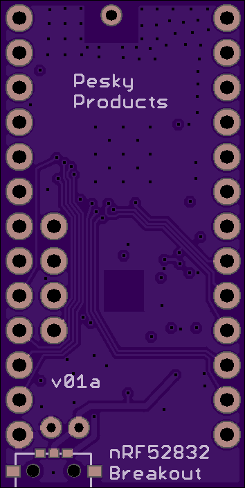
4
layer board of
0.71x1.41
inches
(17.96x35.71
mm).
Shared on
April 25th, 2016 22:56.
Fixed trace error, fixed crystal footprint, reversed Vbat and GND so JST connector can more easily be used, exposed pin 11.