To get your PCB designs manufactured you need to send the pcb manufacturer a bunch of files. These files are called Gerber Files.
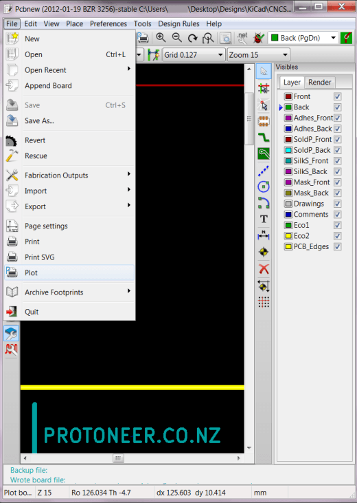
To generate them is easy. When you are done with your design open up your PCB in PCBNew. From the file menu click on “PLOT”.
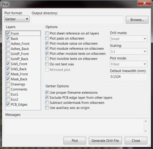
The Plot window is where you will generate the Gerber files from.
- Ensure that the Plot format is set to Gerber.
- It’s useful to set the output directory to a sub-folder. This will separate the Gerber Files from your design files.
- Make sure that PCB_Edges layer is selected.
Description of the files generated:
- GBL File – Gerber Bottom Layer (Bottom copper layer)
- GTL File – Gerber Top Layer (Top copper layer)
- GBR File – Gerber File (Contains the edge lines)
- GBO File – Gerber Bottom Overlay (Bottom Layer silk screen)
- GTO File – Gerber Top Overlay (Top Layer silk screen)
- GBS File – Gerber Bottom Solder Mask
- GTS File – Gerber Top Solder Mask
Once the files have been generated its wise to open them with a Gerber File viewer to make sure they are correct before sending them to the manufacturer. KiCad has a built-in Gerber viewer by the way.
