
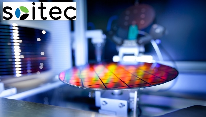
everything RF Interviewed Bernard Aspar, Executive Vice President, Communication & Power Business Unit, Soitec, designer and producer of innovative semiconductor materials that are used in manufacturing electronic components. These materials are substrates onto which the circuits of electronic components are etched and cut. The Company offers new and competitive solutions to pursue the miniaturization of chips, increase their performance and reduce their energy consumption. These products are used to manufacture chips for consumer electronics devices and mobile electronics in smartphones, automotive applications, the Internet of Things (IoT), computer servers and data centers, etc.
Soitec stands out with its technological and industrial expertise in disruptive technologies that are protected by numerous patents. The primary technologies developed by Soitec for the semiconductor market include Smart Cut™, Smart Stacking and epitaxy.
Q. Can you give us a brief history of Soitec?
Soitec was founded in 1992 to develop and commercialize a breakthrough process called Smart Cut™ technology. This is a revolutionary wafer-bonding and layer-splitting process to transfer a thin layer of crystalline material from a donor substrate to another substrate.
Smart Cut™ technology, Soitec’s core technology, is a veritable scalpel on the atomic scale that can be used to transfer ultra-fine monocrystalline layers from a donor substrate to a receiver substrate via ionic implantation and molecular adhesion. It stretches the traditional limits of depositing layers between metals while providing total control of thickness uniformity for layers of silicon and oxide at the atomic mesh. Furthermore, with this technology, donor substrates can be reused and production can be industrialized to serve a wide range of applications. The technology has numerous applications when combined with other Soitec offerings.
Smart Cut™ technology makes it possible to offer integrated circuit manufacturers a competitive alternative to bulk silicon, thanks to performance gains, reduced energy consumption and lower manufacturing costs due to a simplified device architecture.
Soitec’s other technologies and expertise include Smart Stacking™, which is also a layer-transfer technology, but for processed wafers.
Smart Stacking™ technology is a method for transferring wafers onto other materials. It can be used to transfer etched and partially etched wafers onto other components.
For example, it can be used to manufacture silicon transistors and then transfer them onto sapphire, which is more suitable for radio-frequency devices. Finally, this technology makes it possible to use 3D stacking to create several layers of components, thereby increasing the density of the resulting device. It is compatible with a wide range of substrates, which comes into play in producing materials used in the electronic components of back-lit sensors and radio-frequency sensors.
We also have expertise in growing epitaxial layers on compound semiconductor substrates. This technique enables layers of semiconductor materials to be grown on compound semiconductors or insulator substrates.
Our most common engineered substrates currently on the market are silicon-on-insulator (SOI). These substrates enable the fabrication of ICs with higher performance, greater functionalities or lower power consumption cost effectively while also contributing to the advancement of Moore’s Law.
Q. What products do you develop?
We are a world leader in designing and manufacturing innovative semiconductor materials. We use our unique technologies and semiconductor expertise to serve electronics markets. With more than 3,000 patents worldwide, our strategy is based on disruptive innovation to answer our customers’ needs for high performance, energy efficiency and cost competitiveness.
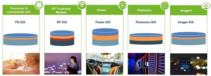
In term of products, we have several SOI product lines available in 200-mm or 300-mm wafer diameters to address different applications.
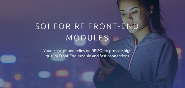
Our radio-frequency SOI (RF-SOI) for RF front-end modules are at the heart of every smart phone manufactured today. The RF-SOI substrates product line enables the best RF switch, LNA, tuner performance, integration and cost for 4G, 5G, and Wi-Fi front-end modules throughout mobile communication markets.
Power-SOI for “smart power” ICs has been used for more than 15 years in mid- to high-voltage driver applications. This product line enables the best reliability, energy-efficiency and cost-effectiveness in transceivers ICs for automotive and industrial markets.
We offer fully depleted SOI (FD-SOI) for processors and connectivity SoCs. To continue the rapid pace of technology advancement, our FD-SOI substrates line enables the best power efficiency, performance and cost for fabricating processors used in mobile, IoT, consumer, automotive and networking markets at the 28-nm and 22-nm technology nodes and beyond.
We also have Photonics-SOI for optical transceivers. With the increase in mobile cloud traffic, the Photonics-SOI substrates product line enables silicon-based optical transceivers with the high data rates and cost-effective optical transmissions required for next-generation data centers and telecommunication networks.
Last but not least, in 2017 we introduced our Imager-SOI product line, which is designed specifically for fabricating front-side imagers for near-infrared (NIR) applications including advanced 3D image sensors.
Q. Can you tell us more about Soitec’s RF-SOI capabilities?
Soitec’s range of RF-SOI products was originally developed to serve the antenna switch market for cellular and Wi-Fi applications. Today, RF-SOI is a design platform for all FEM functions (LNA, Tuner, Passives, and PAs).
A specific feature of RF-SOI products designed and manufactured using Smart Cut technology is a high-resistivity base substrate enabling very low electromagnetic loss. We offer these HR-SOI substrates for the Wi-Fi and 2G-3G Cellular markets. For 4G/LTE Cellular and LTE-Advanced applications, we developed a radio-frequency enhanced signal integrity (RFeSI™) product line, which has a trap rich layer under the buried oxide layer to boost the RF performance.
We cooperate with all players in the RF ecosystem (research centers, bulk substrate suppliers, foundries, RF fabless companies, phone manufacturers, etc.). Our goal is to continuously improve our products’ performance to meet the increasingly demanding specifications of 4G/LTE, LTE-Advanced and future 5G standards for mobile telephony.
Each year, new generations of cell phones are introduced that conform to 4G/LTE, LTE-Advanced, LTE-Advanced Pro and upcoming 5G sub-6-GHz standards. These devices successively ratchet up data-transfer speeds and are now achieving download capacities of 1 Gbit per second. In addition, the number of approved frequency bands for mobile phones has increased from 4 in 2004 to almost 60 today, with each additional frequency band requiring new switches. As a result, more integration and better linearity are required to address this increasing global complexity. These changes are putting greater demands on substrate performance so Soitec is constantly innovating and advancing its range of products to meet these evolving market needs.
As one measure of our success, the RF-SOI technology developed by Soitec currently accounts for more than 90 percent of the market share for antenna switches, according to analysts. This market dominance has led multiple semiconductor manufacturers to add 300-mm RF-SOI production capacity, as announced by GlobalFoundries and Peregrine in July 2015 and TowerJazz in September 2015, with more to come in the near future.
Q. What markets do you cater to? Who are some of your customers?
Soitec’s products and technologies address the increasing demand for rich, diverse online content and enhanced mobility, which is pervading more and more market segments.
For mobile, consumer and IoT applications, Soitec’s products and related technologies help device developers and manufacturers respond to consumer demand for greater performance, longer battery lifetimes and higher integration.
In computing and data communication markets, Soitec provides engineered substrates to support the need for more computing power to accommodate the explosion in online content, increasing data volumes and access from virtually anywhere.
For the automobile and “smart tech” industries, Soitec products address the demand for high reliability, high-voltage operation and highly integrated digital and power functions.
At Soitec, we are working with key fabless companies that are selling or developing SOI-based products. Foundries are our direct customers and we are delivering to all of them.
Q. What is the advantage of SOI wafers over conventional wafers for RF applications?
Traditionally, SOI wafers use standard resistivity silicon as base substrates. For RF FEM applications, the electrical field is diffusing into the base substrate, leading to high-frequency signal losses, non-linearity and crosstalk. To improve the insertion loss, harmonic distortion and isolation performance required, standard resistivity silicon is replaced by a high-resistivity base substrate - typically specified to have resistivity above 1 KOhm-cm - under a thick Box.
The adoption of HR-SOI wafers for RF applications has allowed monolithic integration of RF front-end modules, leading to smaller size, better reliability, improved performance and lower system cost. In this way, RF-SOI wafers enable the device integration, cost effectiveness and high performance needed for high-volume applications. The substrates’ properties allow RF designers to integrate diverse functions such as switches, LNAs, passives, power amplifiers and antenna tuners while providing excellent RF isolation, good insertion loss and better signal integrity at lower cost than traditional technologies.
Because the oxide layer is built at the substrate level, extra process steps such as high-energy implant and conservative design rules are not required on enhanced signal integrity (RFeSI) wafers. And because HR-SOI substrates exhibit excellent RF isolation, designers can integrate diverse functions on the same chip while achieving good insertion loss and better signal integrity than afforded by traditional technologies.
Another major innovation with RFeSI products comes from the ability to accurately predict the RF harmonic distortion performance of the substrate immediately after the RFeSI substrates are fabricated d. This guarantee is provided through the harmonic quality factor (HQF) specification. By meeting some of the most difficult LTE and LTE-Advanced linearity specifications, RFeSI wafers are enabling the next generation of RF standards. Furthermore, these wafers are opening the path to greater power-device integration on SOI by providing better thermal conductivity as well as improving all critical electrical parameters.
Q. Currently where is SOI technology used in the RF and wireless sector?
Perhaps the most apparent RF application of SOI is in smart phones. Almost 100% of smart phones have RF-SOI inside. On average it means more than 20 mm2 of SOI-based circuitry is used in each smart phone built today. That content is projected to increase to 65 mm2 per phone over the next five years.
Q. What factors and technologies do you feel will drive growth in demand for SOI technology?
We are focused on the consumer so the technology must be delivered at the right price with the right performance.
In terms of communications, emerging 5G technology represents an incredible evolution featuring real-time data-transfer speeds. 5G communications will find a huge market in connected cars and autonomous driving, where information from sensors must be conveyed instantaneously to ensure safety.
In order to operate at high frequencies and support high bandwidths, the radio system must provide high performance and power efficiency. To lower the costs and allow full integration of a complete radio System-on-Chip (SoC), it is desirable to integrate the entire transceiver including the digital baseband and the RF in a single chip. When operating at higher frequencies as it becomes hard to meet the stringent requirements in terms of linearity, output power, and power efficiency, FD-SOI can provide many benefits over other technologies.
In other applications, the driving factor will be more performance. For example, in IoT applications, users want products to perform with a level of computing power that demonstrates clear value. But they also want wireless operation and low energy usage for longer battery lifetimes.
These applications play into SOI’s strengths. For SOI to serve such high-volume markets and become part of our everyday lives, we must develop not only the technology, but also the ecosystem. Through several industry initiatives involving suppliers, designers, manufacturers and more, SOI’s global supply chain has been established and is being extended each year.
We are also seeing growth in the market where SOI is already used.
In automotive electronics, today there is about 100 mm2 in SOI circuitry per car and we expect that to grow to 200 mm2 in 5 years.
The cloud is another very interesting application for us. Currently, cloud-related computing systems consume roughly 80 mm2 of SOI devices, growing to 400 mm2 in 5 years.
Q. In addition to RF-SOI wafers, are there any other products you are developing for the RF/wireless segment?
Yes, we are always working on designing and developing new substrates. For instance, we are currently developing a new engineered substrate for filters, which comprise 50 percent of the RF content in smart phones. To get more data, you need more bands. As the number of bands increases, filters’ capabilities must increase. So we have developed a new generation of piezoelectric-on-insulator substrates. They have a new structure, in which a thin monocrystalline layer of piezoelectric material is bonded on a silicon wafer through an oxide. This structure provides temperature stability to build multi frequency filters that support wide bands and enable further integration, reducing overall cost. This technology, currently under evaluation by some customers, will allow us to offer products for the full range of front end modules.
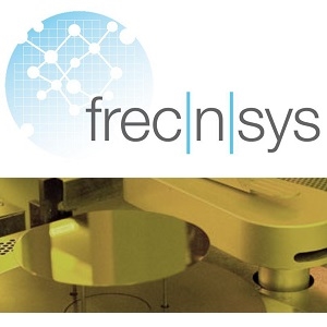
To help develop this product, we recently acquired a spin off from the University of Besançon in France called frec’n’sys. The company has experts in piezoelectric materials from sensor design and prototyping small products as well as a characterization lab. We made the acquisition to accelerate the adoption of piezoelectric-on-insulator substrates, to explore opportunities to build some new kinds of sensors with this substrate and to better understand the design and modelling for filters. This extends our leadership position in delivering solutions with SOI.
Q. Where are your manufacturing plants located? What products are produced in each plant?
Based in France, next to Grenoble and the French Alps, Soitec has the world’s largest SOI industrial production site. It includes a total of 4,500 square meters of cleanrooms located in three facilities. This is where we manufacture 200-mm products such as RF-SOI and Power-SOI (with a capacity of 850,000 wafers per year) and, in our 300-mm fab (with a capacity of 650,000 wafers per year), our FD-SOI, Photonics-SOI, Imager-SOI products. We also began manufacturing 300-mm RF-SOI substrates in response to market demand. Our third fab is dedicated to producing non silicon semiconductor substrates.
In addition, we have a 300 mm manufacturing plant in Singapore that we just re-opened. When fully equipped, it will have a capacity of 800 000 wafers.
We also have a partnership with the Chinese company Simgui based in Shanghai manufacturing 200-mm SOI wafers using Soitec’s Smart Cut technology. This partnership is important for us in managing our worldwide production capabilities. Our manufacturing partner in China significantly increases our production capacity in 200-mm SOI wafers to meet growing worldwide demand and, at the same time, represents a key step in establishing a SOI ecosystem in China.